High Speed Switching with Low Capacitances
High Blocking Voltage with Low On-Resistance
Easy to Parallel and Simple to Drive
Avalanche Ruggedness
Halogen Free, RoHS Compliant
Benefits:
Higher System Efficiency
Reduced Cooling Requirements
Increased Power Density
Increased System Switching Frequency
Maximum Ratings (Tc = 25°C unless otherwise specified)
| Parameter | Symbol | Value | Unit | Test Conditions | Note |
| Drain-Source Voltage | VDSmax | 1200 | V | VGS = 0 V, ID = 100 μA | |
| Gate-Source Voltage | VGSmax | -0.421052632 | V | Absolute maximum values | |
| Continuous Drain Current | ID | 32 | A | VGS = 15 V, TC = 25˚C | Fig.19 |
| 23 | VGS = 15 V, TC = 100˚C | ||||
| Pulsed Drain Current | ID(pulse) | 80 | A | Pulse width tP limited by Tjmax | Fig.22 |
| Power Dissipation | PD | 273 | W | TC =25˚C, TJ =175˚C | Fig.20 |
| Operating Junction and Storage | TJ , Tstg | -55 to | ˚C | ||
| Temperature | +175 | ||||
| Solder Temperature | TL | 260 | ˚C | 1.6mm (0.063”) from case for 10s | |
| Mounting Torque | Md | 1 | Nn | M3 or 6-32 screw | |
| 8.8 | lbf-in |
Electrical Characteristics (Tc = 25°C unless otherwise specified)
| Parameter | Symbol | Min. | Typ. | Max. | Unit | Test Conditions | Note |
| Drain-Source | V(BR)DSS | 1200 | - | V | VGS = 0 V, ID = 100μA | ||
| Breakdown Voltage | |||||||
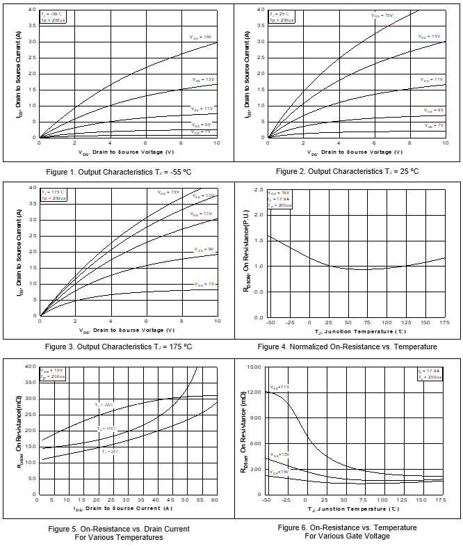
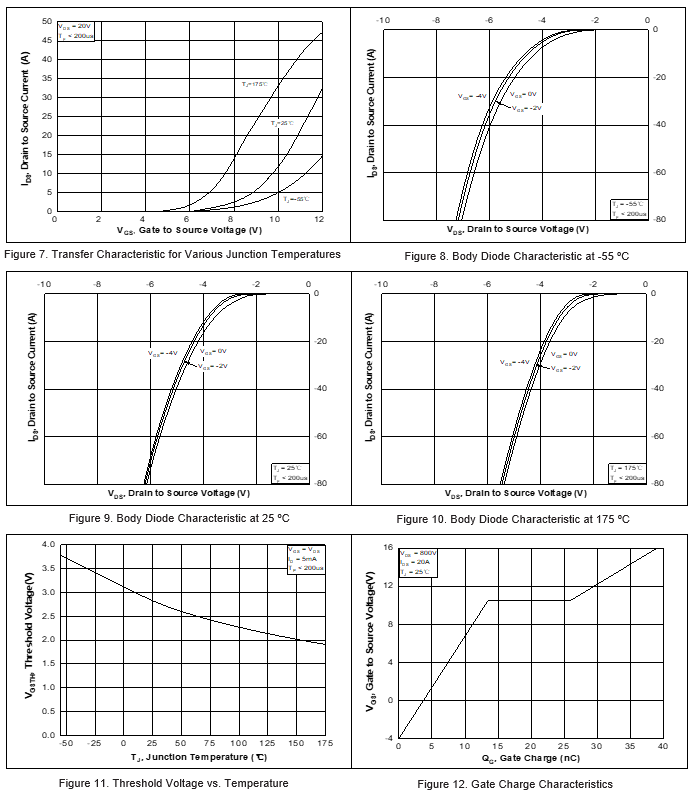
| Gate threshold Voltage | VGS(th) | 1.8 | 2.8 | 3.6 | V | VDS = VGS, ID = 5mA | Fig.11 |
| 1.9 | V | VDS = VGS, ID = 5mA, TJ=175°C | |||||
| Zero Gate Voltage Drain Current | IDSS | 1 | 50 | μA | VDS = 1200 V, VGS = 0 V | ||
| Gate Source Leakage Current | IGSS | 10 | 250 | nA | VGS = 15V, VDS = 0 V | ||
| Drain-Source | RDSON | 90 | mΩ | VGS = 20 V, ID = 20A | Fig.4.5.6 | ||
| On-State Resistance | 85 | VGS =20 V, ID = 10A | |||||
| Transconductance | gfs | 5.1 | S | VDS = 20 V, ID = 17.9A | Fig.7 | ||
| 5.7 | VDS = 20 V, ID = 17.9A, TJ=175°C | ||||||
| Input Capacitance | Ciss | 1180 | pF | VGS=0V,VDS=1000V, | Fig.17,18 | ||
| Output Capacitance | Coss | 61 | TJ=25°C,f=1MHz, | ||||
| Reverse Capacitance | Crss | 2.9 | VAC = 25mV, | ||||
| Coss Stored Energy | Eoss | 36 | μJ | Fig.16 | |||
| Effective Output Capacitance (Energy Related) | Co(er) | 307 | pF | VGS = 0 V, VDS = 0... 800V | |||
| Effective Output Capacitance (Time Related) | Co(tr) | 222 | pF | ||||
| Turn on Switching Energy | Eon | 367 | μJ | VDS = 800 V, VGS = -4/15 V, | Fig.26,29 | ||
| Turn off Switching Energy | Eoff | 97 | ID = 20A, RG(ext) =2.5Ω,L=135μH | ||||
| Turn on delay time | tdon | 26 | ns | VDS = 800 V, VGS = -4/15V, | Fig.27,28 | ||
| Rise time | tr | 20 | ID =20A, RG(ext)= 2.5Ω,L=135μH | ||||
| Turn off delay time | tdoff | 13 | |||||
| Fall time | tf | 8.3 | |||||
| Internal Gate Resistance | Rgint | 3.4 | Ω | VAC=25mV, f=1MHz | |||
| Gate to Source Charge | Qgs | 13 | nC | VDS = 800 V, VGS = -4/ 15 V, | Fig.12 | ||
| Gate to Drain Charge | Qgd | 13 | ID = 20A | ||||
| Total Gate Charge | Qg | 39 |
Electrical Characteristics (Tc = 25°C unless otherwise specified)
| Parameter | Symbol | Min. | Typ. | Max. | Unit | Test Conditions | Note |
| Diode Forward Voltage | VSD | 3.8 | 7 | V | VGS = -4 V, ISD = 9A | Fig.8,9,10 | |
| 3.4 | VGS = -4 V, ISD = 9A,TJ=175°C | ||||||
| Continuous Diode Forward Current | IS | 32 | A | VGS = -4 V,Tc=25°C | |||
| Diode pulse Current | IS,pulse | 80 | A | VGS = -4 V,Pulse width tp limited by Tjmax | |||
| Reverse Recovery Time | trr | 56 | ns | VGS= -4 V,VR= 800 V, ID = 20A, di/dt=885A/μs,TJ=175°C | |||
| Reverse Recovery Charge | Qrr | 370 | nC | ||||
| Peak Reverse Recovery Current | Irrm | 10.4 | A | ||||
| Reverse Recovery Time | trr | 57 | ns | VGS = -4V, VR= 800 V, ID = 20A, di/dt=740A/μs,TJ=175°C | |||
| Reverse Recovery Charge | Qrr | 370 | nC | ||||
| Peak Reverse Recovery Current | Irrm | 10 | A |
Thermal Characteristics
| Symbol | Parameter | Value | Unit | Note |
| RɵJC | Thermal Resistance(Junction to Case) | 0.55 | °C/W | Fig.21 |
| RɵJA | Thermal Resistance From Junction to Ambient | 27 |
Typical Performance
Attention
Specifications of any and all products described or contained herein stipulate the performance, characteristics, and functions of the described products in the independent state, and are not guarantees of the performance, characteristics, and functions of the described products as mounted in the customer’s products or equipment. To verify symptoms and states that cannot be evaluated in an independent device, the customer should always evaluate and test devices mounted in the customer’s products or equipment.
We assumes no responsibility for equipment failures that result from using products at values that exceed, even momentarily, rated values (such as maximum ratings, operating condition ranges, or other parameters) listed in products specifications of any and all Silicon products described or contained herein.
Any and all information described or contained herein are subject to change without notice due to product/technology improvement, etc.